
Intel said Monday it is completely changing the way in which generations of its microprocessors have been defined, discussed, and evaluated, paving the way for chips to be measured in angstroms, not nanometers.
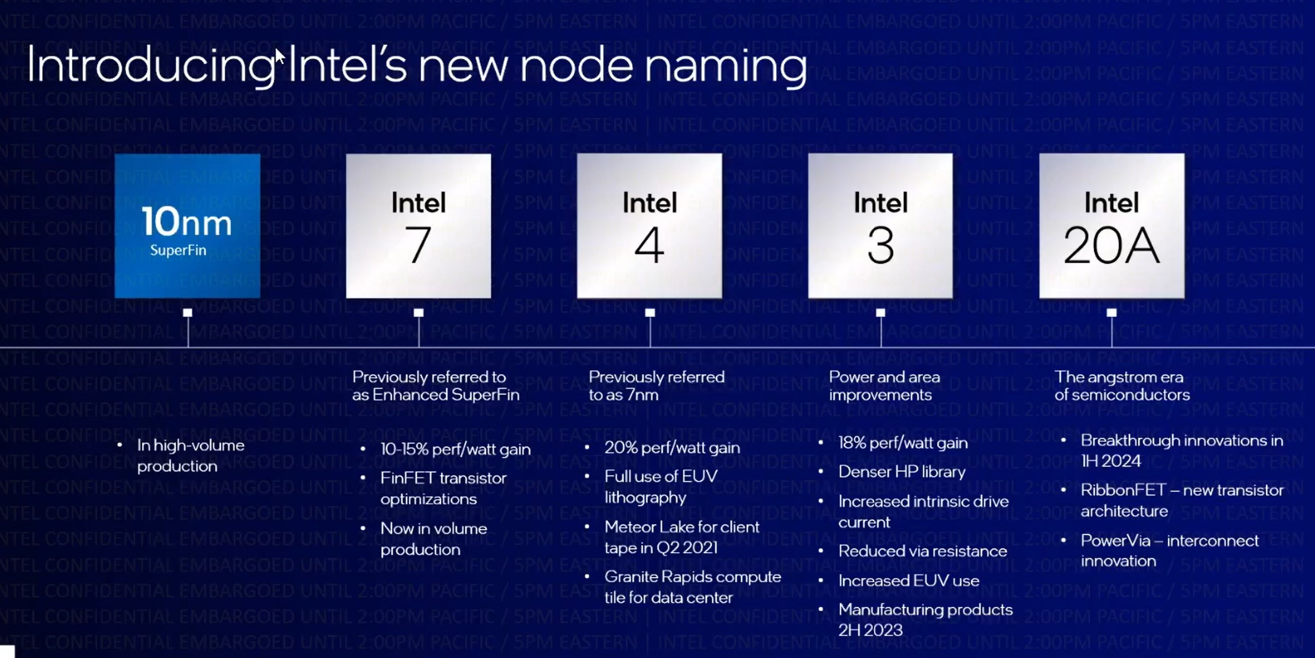
Specifically, Intel is rewriting the terminology associated with its process technology, it said at an “Intel Accelerated” presentation. Going forward, Intel’s 10nm “enhanced SuperFIN” technology will now be called “Intel 7,” mentally placing it on the same tier as the same 7nm process technology AMD uses for its Ryzen chips. Intel began signaling this shift in March, but today it’s official.
It’s a branding exercise, but with technical reasons behind it. For years, one way in which chip giants like Intel and AMD have defined the evolution of their products has been through process nodes or process generations: first in terms of microns, then nanometers, such as the 14nm process Intel has struggled to move past. But what defines a “7nm” process has become increasingly abstract, to the point at which some, like Intel, would argue that the term has become essentially meaningless. Instead, Intel will distinguish process nodes by a new metric: performance per watt.
Intel’s announcement on Monday includes three important components. For one, Intel is simply abandoning the traditional way of defining new process nodes, changing the way in which you’ll talk about its products. Second, the announcement charts the end of the “nanometer” era, and looks forward to defining chips based on angstroms. Finally, Intel’s made a bold claim that it will regain what it calls manufacturing leadership by 2025.
 Intel
IntelThe “old way” of defining Intel’s manufacturing process: using microns and nanometers.
The new language of Intel’s chip manufacturing
Intel’s manufacturing technologies will now be known as “Intel 7,” “Intel 4,” “Intel 3,” and then—moving on—“Intel 20A.” They will be primarily defined by how much they improve in performance per watt from the prior generation. An Intel representative added that they will also be defined with an “area improvement as a key technical parameter,” but said that the company wouldn’t be providing those numbers.
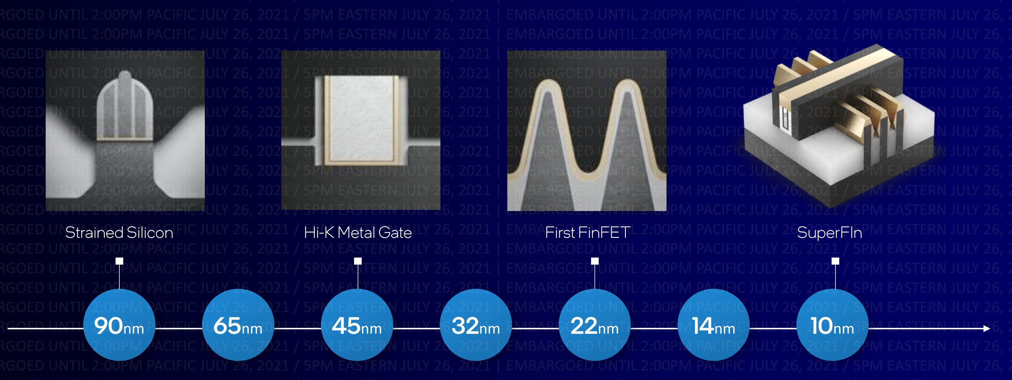
Traditionally, what we call the “process node” or “process technology” was just the length of the individual transistor gate, the fundamental building block of integrated circuits. As semiconductor manufacturing improved, the sizes of the individual gates shrank. That enabled Moore’s Law: the axiom that the number of transistors in a fixed area on a chip doubles every 18 to 24 months. But as ExtremeTech noted in a 2019 story, the last time that the gate length matched the process node was way back in 1997. Instead, over time, chipmakers began essentially replacing “actual” gate lengths with “equivalents,” as the ways to compare manufacturing processes became increasingly complex, involving SRAM cell sizes, fin width, minimum metal pitch, and more. None of these factors, however, are ever used in general conversation.
Now, however, this will be the language Intel uses to talk about new process nodes:
 Intel
IntelIntel’s new manufacturing lexicon: Intel 7, Intel 4, and Intel 3.
Intel’s 10nm “SuperFIN” technology will be referred to as just that. But the “Enhanced SuperFIN” technology used within the upcoming Alder Lake chip will now be called simply “Intel 7,” and defined as simply 10 percent to 15 percent more efficient in performance per watt. Dr. Sanjay Natarajan, Intel’s senior vice president and co-general manager of Intel’s Logic Technology Development, said the relationship isn’t totally uniform: At a fixed power, Intel 7 performance will increase by 10 to 15 percent, as expected. But at a fixed performance, Intel can lower power by more than that, he said.
Below, we’ve summarized each new process node, along with a representative processor and the expected timing.
Intel 10nm SuperFIN: In production. Example: Intel’s 11th-gen “Tiger Lake”
Intel 7 (Intel 10nm Enhanced SuperFin): In production, with 10-15 percent more performance/watt than the prior generation. Example: “Alder Lake”
Intel 4 (Intel 7nm): Q2 2021 tapeout, with 20 percent more performance/watt than the prior generation. Example: “Meteor Lake,” “Grand Rapids” (Xeon)
Intel 3: 2H 2023, with 18 percent more performance/watt than the prior generation. Example: Not yet announced
Intel 20A: 1H 2024. No further details at this time
Intel 18A: 2025. No further details at this time
According to Dr. Ann Kelleher, senior vice president and co-general manager of Intel Logic Technology Development, Intel’s changes were in response to “feedback we’ve gotten over the years,” and that this new framework is being set up “so that it can be clear, consistent and meaningful.”
Recall that in March, Intel’s new chief executive, Pat Gelsinger, announced IDM 2.0: a strategy to improve Intel’s competitiveness by investing in new fabs, improved manufacturing technology, and an entirely new foundry business that will manufacture chips for other companies, including integrating Intel’s CPUs. One would expect that Intel will provide these customers the technical detail that it’s publicly shying away from.
On to angstroms
Angstroms are simply the next unit of measurement in semiconductors, from microns to nanometers to angstroms—an angstrom is 0.1 nm. While Intel isn’t measuring anything in angstroms, it’s using the term “angstrom” to highlight its next manufacturing generation.
As Intel continues to step forward on its roadmap, Intel plans increased usage of EUV (extreme ultraviolet) lithography—a manufacturing technique that has become necessary as more conventional lithography runs out of steam. Here’s the problem: The details of semiconductors have become too small compared to the wavelengths of laser light that carves them out. Chipmakers found ways to “cheat” using techniques called patterning, but the process simply became too complex to continue.
EUV, however, has its own challenges. For one, the process will probably require more power than traditional lithography. But EUV also requires a vacuum, because EUV radiation is absorbed by solid matter of all types. So-called random stochastic effects, which can cause manufacturing errors, have also been a challenge with EUV manufacturing. Intel has been able to get around that with innovations like its “F” series Core chips, where errors that can kill its integrated GPUs are instead sold with those GPUs turned off.
EUV will be required to move into the angstrom generation, but there will be some real questions as to Intel’s manufacturing costs—and chip prices—over the next few years. Balance that against an ongoing chip shortage, and there are reasons for some butterflies in the stomachs of PC customers, especially with Intel already warning of chip shortages.
A new Intel transistor: RibbonFET
Intel said this new generation will be accompanied by innovations in transistor manufacturing and packaging, including its first transistor redesign since it announced its stacked FinFET technology in 2011.
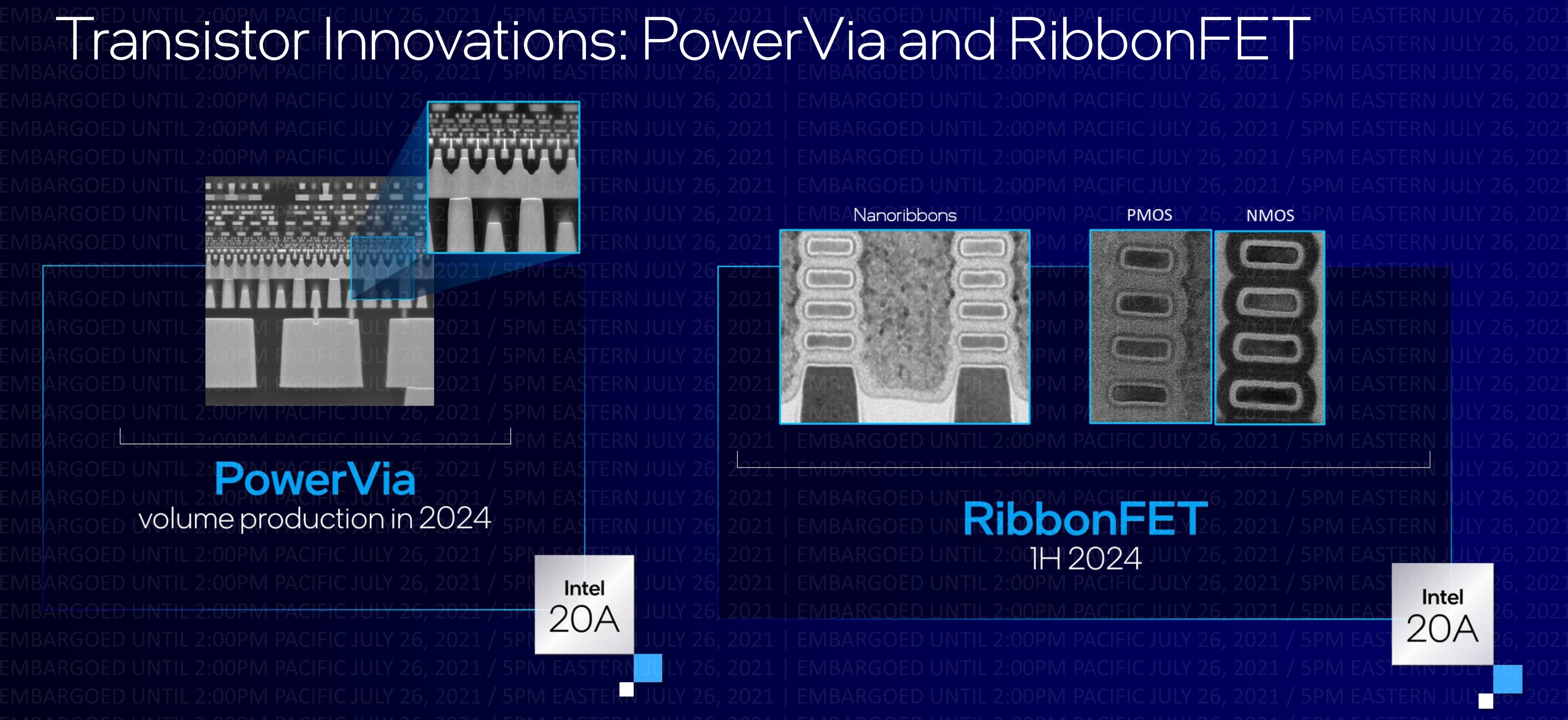 Intel
IntelIntel’s new PowerVia and RibbonFET technologies.
Here, Intel is making two more shifts: moving the power vias, or transports, from the top to the bottom of the chip; and moving to a “gate all around” (GAA) design, or RibbonFET. The PowerVia technology, as it’s known, will improve power efficiency, Natarajan said. “Gate-all-around” essentially creates nanowires through the chip. (A Lam Research blog explains GAA a bit more.) Both the PowerVia and RibbonFET technology will be part of Intel 20A, in 2024.
What GAA does is further extend chip design from two to three dimensions. That’s been the direction in packaging, too. Intel announced the Embedded Multi-die Interconnect Bridge, or EMIB, in 2017. That allowed Intel CPUs to be constructed from different processor dies within the same chip. The Foveros technology allowed for those different dies to be stacked vertically. That evolved into the slow, prototypical Lakefield chip, part of the Samsung Galaxy Book S. But Intel is expected to use the two technologies inside the upcoming Alder Lake and Meteor Lake chips, as well.
 Intel
IntelIntel’s Foveros Omni and Foveros Direct packaging technologies.
What Intel is calling Foveros Omni will extend that further. Foveros Omni will take what’s called the “die disaggregation” portion of Foveros and extend that vertically—basically, it will give Intel more tools to mix and match performance cores and low-power cores together inside of the same chip. A second technique, called Foveros Direct, will add direct copper-to-copper bonding for even lower electrical resistance, and thus performance.
It’ll be in 2024, with the Intel 20A process, when this all comes to fruition, Intel says. By the following year, in 2025, Intel believes it will move back into leading the industry in manufacturing. “We’re already working on 18A, which I’m not going to get to details on,” Natarajama said. “The timeframe we believe we will be in a technology leadership position is by 2025, with our 18A technology.”
Stay connected with us on social media platform for instant update click here to join our Twitter, & Facebook
We are now on Telegram. Click here to join our channel (@TechiUpdate) and stay updated with the latest Technology headlines.
For all the latest Technology News Click Here
For the latest news and updates, follow us on Google News.